Mosfet Type on Laptop Motherboard
There are 4 type of mosfet’s SO8 on laptop motherboard
1. P channel mosfet
2.N chanel mosfet
3.dual P channel mosfet
4.Dual N chanel mosfet
each type could substitute as long as same type even with different marking code.
Easy way to identified look at the end number of marking code .
example :
AO 4433 look at end of marking code number is odd numbers ( 3 )
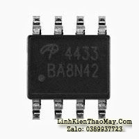
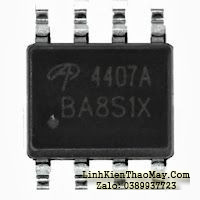
this is P channel
example : AO 4407 (7) is odd number ,this is P channel too,
they could be substitute each other even different manufacture and code.
Others P chanel examples :
AF 4825-AM 3423-FDS 6679-SI 4835 ETC
Other example : AOD 4466
look at last number of marking code it is even (6) numbers it’s mean this is N channel mosfet and they could replace by other N channel even different
manufacture and code .
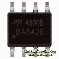
Others N channel mosfet examples: AO 4800
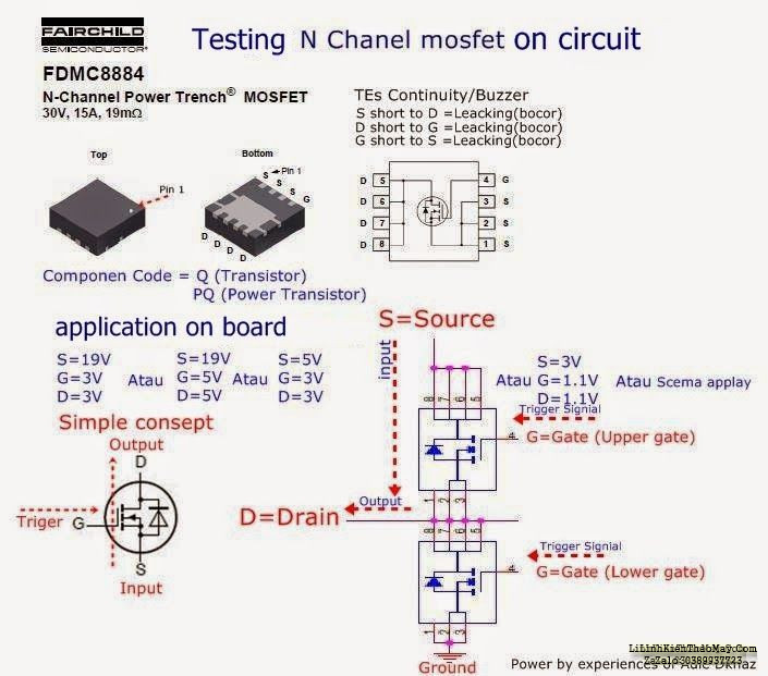
AO 4474-AP 4232-FDMC8844-SI 4812 ETC
those mosfet identified only for SO8 mosfet.
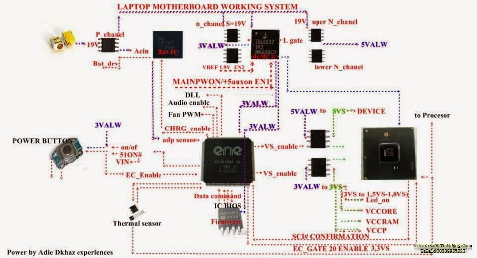
We can see P channel mosfet function on this “GENERAL LAPTOP MAIN POWER “ layout link :

There are only 3 pcs P channel there ,2 pcs ADP(adapter) fet’s and 1pcs Bat (battery)fet .some
motherboard also may have 1 adp Fet,some replace with diodes to supply every adapter supply need.
I call it “VALW MAIN LINE” .from this line Battery ic and dc/dc power supply ic get VCC to powered each ic and this main VALW line also distributed adapterVoltage to every N channel Source ,before they got enable trigger to produced 3 and 5V_ALW……
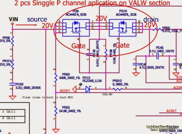
P-channel mosfet works drain is a input for nagative supply and source is a output for nagative supply ,and it’s gate on with nagative volt .same way if you want to drive positive supply from p-channel mosfet then souce is input and drain is output for positive supply .
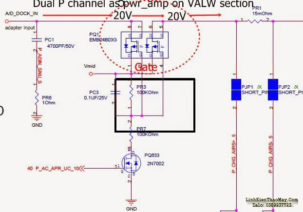
This is How 2 pcs P chanel replace by 1 Dual P chanel Mosfet
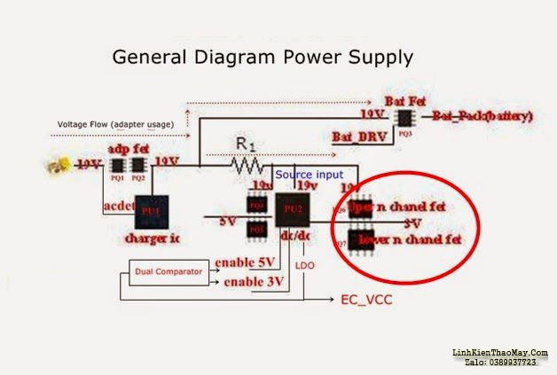
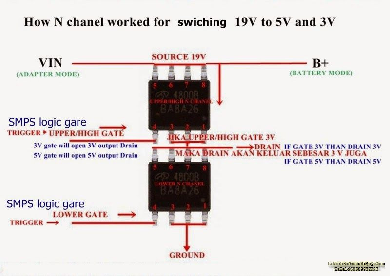
Look at this lay out function N channel mosfet as integrated circuit with DC/DC main power supply to produce 3V and 5V_ALW in this link :
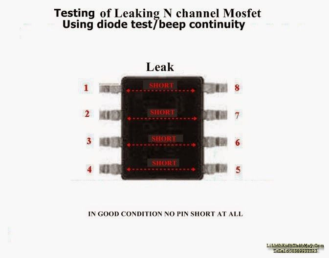
and what happen if P or N channel leak and what if suppose N channel replace with and P channel and what damage it could be on this link:
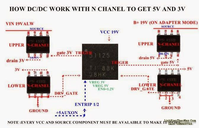
How DC/DC main power supply open/close gate N channel to produce 3V and 5V_ALW and important signal enable/disable function to activate the DC/DC main supply ic (ISL 6237-RT 8206-TPS 51247) on this link:
How do (RT8223-TPS 51125-TPS 51123)work and signal need on this link :
If you confused ,you should read this before
Introduction of System Power Laptop Motherboard in this link
and to avoid accident before repairing you shoul read
THINGS THAT SHOULD NOT BE TAKEN IN MOTHERBOARD REPAIR
We will also found (SO3) P channel ,(SO8) mean mosfet have 8pin and (SO)3 mean they
have 3 pin.And this (SO3) also have P or N channel type .so be ware if you
want to make replacement .just make sure replace it whit same type .
Other way to Identified for (SO6) and (SO3) Mosfet transistors are by finding the marking code on ic than
browse the data sheet , if they not found get mosfet location code on board than
find on schema by typing marking code to adobe reader search column to look the correct marking code than browsing the datasheet again to get know mosfet type and get substitution…
this is one of sample N channel (SO3) code : 2N7002 -P0603BDG
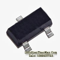
samples (SO3) P channel mosfet :
FDD6685 – SI12301 -TP0610K.
sample datasheet link for N channel (SO3) 2N7002 : https://www.fairchildsemi.com/ds/2N/2N7000.pdf
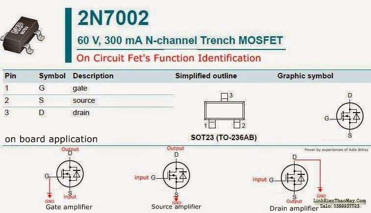
n-channel mosfet voltage flow is drain to source for positive supply – when you apply + positive volt in gate then this mosfet drive voltage drain to souce ( gate works same as transister base) if you want to drive nagative volt from n-channel mosfet then nagative volt drive source to drain mean for nagative volt input is source and output is drain
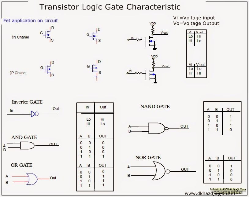
n channel mosfet logic low (vi) that mean mosfet not close circuit between the drain and source ,v_out you got vdd voltage via resistance . (Hi)
when you apply vi = Hi in N-Channel mosfet ,mean drain to source connected (close circuit) in this case you got v_out source low you can got at v_out .same way in P-channel but gate work reverse as n-channel mosfet work
There are 4 type of mosfet’s SO8 on laptop motherboard
1. P channel mosfet
2.N chanel mosfet
3.dual P channel mosfet
4.Dual N chanel mosfet
each type could substitute as long as same type even with different marking code.
Easy way to identified look at the end number of marking code .
example :
AO 4433 look at end of marking code number is odd numbers ( 3 )


this is P channel
example : AO 4407 (7) is odd number ,this is P channel too,
they could be substitute each other even different manufacture and code.
Others P chanel examples :
AF 4825-AM 3423-FDS 6679-SI 4835 ETC
Other example : AOD 4466

look at last number of marking code it is even (6) numbers it’s mean this is N channel mosfet and they could replace by other N channel even different
manufacture and code .

Others N channel mosfet examples: AO 4800
AO 4474-AP 4232-FDMC8844-SI 4812 ETC
those mosfet identified only for SO8 mosfet.
We can see P channel mosfet function on this “GENERAL LAPTOP MAIN POWER “ layout link :

There are only 3 pcs P channel there ,2 pcs ADP(adapter) fet’s and 1pcs Bat (battery)fet .some
motherboard also may have 1 adp Fet,some replace with diodes to supply every adapter supply need.
I call it “VALW MAIN LINE” .from this line Battery ic and dc/dc power supply ic get VCC to powered each ic and this main VALW line also distributed adapterVoltage to every N channel Source ,before they got enable trigger to produced 3 and 5V_ALW……

P-channel mosfet works drain is a input for nagative supply and source is a output for nagative supply ,and it’s gate on with nagative volt .same way if you want to drive positive supply from p-channel mosfet then souce is input and drain is output for positive supply .
This is How 2 pcs P chanel replace by 1 Dual P chanel Mosfet

Look at this lay out function N channel mosfet as integrated circuit with DC/DC main power supply to produce 3V and 5V_ALW in this link :

and what happen if P or N channel leak and what if suppose N channel replace with and P channel and what damage it could be on this link:

How DC/DC main power supply open/close gate N channel to produce 3V and 5V_ALW and important signal enable/disable function to activate the DC/DC main supply ic (ISL 6237-RT 8206-TPS 51247) on this link:

How do (RT8223-TPS 51125-TPS 51123)work and signal need on this link :

If you confused ,you should read this before
Introduction of System Power Laptop Motherboard in this link

and to avoid accident before repairing you shoul read
THINGS THAT SHOULD NOT BE TAKEN IN MOTHERBOARD REPAIR
We will also found (SO3) P channel ,(SO8) mean mosfet have 8pin and (SO)3 mean they
have 3 pin.And this (SO3) also have P or N channel type .so be ware if you
want to make replacement .just make sure replace it whit same type .
Other way to Identified for (SO6) and (SO3) Mosfet transistors are by finding the marking code on ic than
browse the data sheet , if they not found get mosfet location code on board than
find on schema by typing marking code to adobe reader search column to look the correct marking code than browsing the datasheet again to get know mosfet type and get substitution…
this is one of sample N channel (SO3) code : 2N7002 -P0603BDG

samples (SO3) P channel mosfet :
FDD6685 – SI12301 -TP0610K.
sample datasheet link for N channel (SO3) 2N7002 : https://www.fairchildsemi.com/ds/2N/2N7000.pdf


n-channel mosfet voltage flow is drain to source for positive supply – when you apply + positive volt in gate then this mosfet drive voltage drain to souce ( gate works same as transister base) if you want to drive nagative volt from n-channel mosfet then nagative volt drive source to drain mean for nagative volt input is source and output is drain

n channel mosfet logic low (vi) that mean mosfet not close circuit between the drain and source ,v_out you got vdd voltage via resistance . (Hi)
when you apply vi = Hi in N-Channel mosfet ,mean drain to source connected (close circuit) in this case you got v_out source low you can got at v_out .same way in P-channel but gate work reverse as n-channel mosfet work
